Tunable Metamaterials in the Infrared
ABSTRACT
Metamaterials are synthetically engineered materials that can bend and manipulate light in unnatural ways. While most metamaterials are passive with properties that cannot be tailored once they are fabricated, the integration of active media enable metamaterials with tunable optical properties, which can be used in a variety of applications such as holograms, signal processing, beam-splitting, flat lenses, and displays. Vanadium dioxide (VO2) is an inorganic compound that undergoes a structural and electronic phase change around 67 ℃, accompanied by a dramatic change in its optical properties in the infrared spectrum. The low temperature phase change allows for a low power threshold and thermal load, making this material an optimal choice for integration with metamaterials. An infrared tunable metamaterial was achieved in this work by adding VO₂ to gold resonators. The metamaterial, based on gold plasmonic resonators, was designed and created using photolithography, followed by VO₂ film deposition and annealing. By measuring infrared reflection spectra, the VO₂ material was confirmed to change from a semiconductor to a conductor and offers a route towards reflection modulation of approximately 20% in the infrared. This design is a candidate for dynamic metamaterials in applications like perfect reflection, nanoguiding, subwavelength focusing, infrared camouflage, and cloaking.
INTRODUCTION.
Electromagnetic metamaterials are synthetically engineered materials that can bend and manipulate light in unnatural ways [1]. By designing unit cells that act as artificial atoms, metamaterials can be created with abnormal properties like negative refractive index, reverse Doppler effect, and sub-wavelength focusing. Since the unit cells are smaller than the wavelength of light being used, the metamaterial acts as a homogenous material. These unique materials can also be used for ultrathin lenses, perfect absorbers, cloaking, and holography [1-3]. While typical lenses are limited by the material used and the feasible curvature of the material, the use of metamaterials allows for the realization of ultrathin lenses because the phase of the light is being manipulated by the unit cells, not by the curvature of the material. Metamaterials can also be constructed with non-periodic unit cells, causing light to bend around objects and resulting in invisibility.
Metamaterials are often designed with periodic patterns of multiple elements to create uniform properties and are sometimes composed of super-cells to achieve abnormal bending or refraction. Metamaterials are usually passive, or cannot be changed after they are created, restricting the possible applications. However, active metamaterials can change states or properties with the use of stimuli like temperature or electricity, which allows for multiple types of light manipulation within one structure. Using active components in metamaterials allows for properties to be modulated after fabrication, which makes these active metamaterials applicable for a wider range of applications. Liu et al used vanadium dioxide (VO2) on a sapphire substrate to create a phase shifting metamaterial and used gold on a VO2 film to create a metamaterial that transitions from insulator to metal [4]. Wei et al used VO2 on a silicon dioxide (SiO2) substrate to create a metamaterial that switches optically and electrically [5]. Non-metamaterial nanostructures are typically restricted by fabrication limits, minimizing the use in many applications [6, 7].
In this project, an active material controlled by temperature, VO2, was added to a plasmonic metamaterial to make a tunable metamaterial in the infrared. Plasmonic, or metallic, metamaterials are one particular variant of metamaterials that function by taking advantage of surface plasmons. Plasmonic metamaterials result in strong light concentration near the surface, which is one of the reasons they are ideal for applications such as light concentrators, near-field scanning optical microscopy, photodetectors, modulators, signal-processing, nanoguiding, and sensors [6, 7]. VO2 is an inorganic compound that experiences a phase change at 67 ℃, which results in a drastic change to both its electrical and optical properties. It has been used in many metamaterials for applications such as signal intensity modulation, phase control, or polarization control [4, 8, 9]. When heated, VO2 undergoes a semiconducting to metallic transition. In the metallic state, the VO2 is also much more absorbing. It is often used in thin layers or films, but the thickness can be varied based on the intended modulation depth [10].
In this paper, the reflection spectra of a tunable metamaterial formed from gold resonators with surrounding VO2 is optically characterized as a function of temperature. The reflection changes in the infrared as a function of temperature are the focus of the characterization. The ability to change optical properties in the infrared could lead to faster communication with lower energy consumption, holograms, beam steering, spatial light modulators, tunable perfect absorbers, infrared camouflage, and active cloaking [1-3, 6, 7, 11].
MATERIALS AND METHODS.
Simulations.
The dimensions for the metamaterial were determined using computer simulations. For the simulations, CST Microwave Studio was used to design and optimize a plasmonic resonator. A silicon substrate with a refractive index of 3.4 was chosen in this simulation to match the experiments. Gold was chosen since it is nearly lossless in the infrared. In the simulation, a Drude model was used to simulate the gold properties with the plasma frequency set to 2.06e15 s-1 and collision frequency set to 1.09e13 s-1. The metamaterial was simulated with a periodic boundary condition, and the unit cell was subjected to an atmospheric environment to mimic experimental conditions. The diameter was set to 4 µm and the lattice constant was set to 6 µm to target operation in the mid-infrared.
Photolithography.
Gold plasmonic resonators were made on a silicon substrate using photolithography (Figure 1). Photolithography allows for microscale structures to be fabricated while also allowing relatively large-scale samples, up to multiple centimeters, to be created, making it a better choice than electron beam lithography. An array size of 6 mm x 6 mm was targeted here. After cleaning, the wafer was coated with positive photoresist (Shipley 1813), spinning at 6000 rpm for 45 seconds, followed by a two-minute soft bake at 90 ℃ to eliminate the solvent (Figure 1). This resulted in a photoresist with a thickness of approximately 1 µm. An ultraviolet laser writer was used to expose the resonator pattern into the photoresist (Figure 1). The laser was calibrated to be 25 mW with pulse duration percentage at 50%. After exposure, the sample was immediately soaked in developer (MF 319) for 1 minute to remove the exposed portions of the photoresist (Figure 1). Chromium and gold films were then thermally deposited over the entire sample with a thickness of 3 nm and 100 nm, respectively (Figure 1). After deposition, the sample was soaked in acetone for 4 hours at 60 ℃ to remove all the photoresist and the metal film on top (Figure 1). Only the patterned gold plasmonic resonators remained on the silicon substrate. The VO2 film, with a thickness of 100 nm, was grown on the top of the gold pattern using radio frequency sputtering followed by rapid thermal annealing.
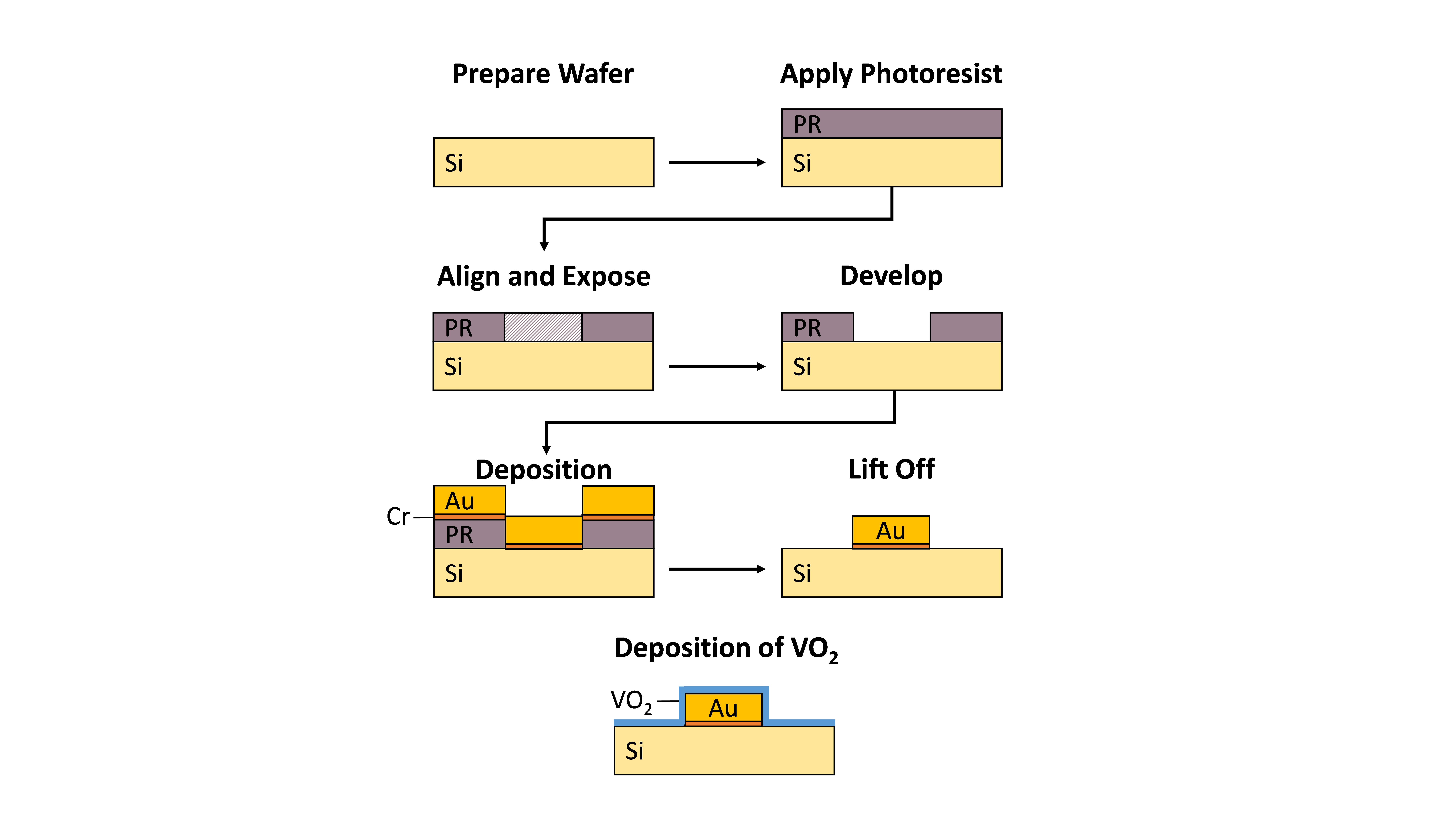
Figure 1. Overview of the photolithography process employed. The wafer is cleaned to remove possible contaminants and to increase adhesion with the photoresist. The photoresist is applied evenly with spin coating. The mask is aligned to ensure accuracy of the pattern being transferred. The photoresist is exposed to ultraviolet light to change solubility and then is developed. The desired material is deposited over the photoresist. The material on top of the photoresist is removed, leaving only the final pattern. The VO2 is deposited in a uniform, 100 nm layer over the final gold pattern to create the final metamaterial.
Fourier Transform Infrared Spectroscopy.
The reflection of both the gold resonator on a silicon substrate and the gold resonator with surrounding VO2 on a silicon substrate was measured in the infrared to identify the resonant wavelengths and to identify the peak reflection. Fourier Transform Infrared Spectroscopy (FTIR) was used because it allows for reflection and transmission spectra measurements in the infrared. FTIR was used to measure the reflectance of the gold resonators without surrounding VO2 and gold resonators with surrounding VO2 as a function of wavelength with a gold mirror used as a reference. The gold resonator with surrounding VO2 was measured at 21.4 °C and at 85.6 °C, respectively, to ensure both the semiconductor and metal states were completely reached. The two VO2 spectra were compared to determine if the peak reflection and resonant wavelength were tunable with temperature. The experimental data was also compared to the simulated results.
RESULTS.
Scanning Electron Microscopy.
A scanning electron microscope (SEM) was chosen to image the nanoscale structures due to its capability to obtain high resolution pictures at the nanoscale. Each unit cell was composed of a disk with a diameter measured to be approximately 4 µm and a lattice constant measured to be approximately 6 µm (Figure 2A and 2B). The images show that the resonators are circular, with minor imperfections present only on the edges of the array due to fabrication limitations. A magnification of 1000x was used in Figure 2A and a magnification of 3000x was used in Figure 2B. Both SEM images show the gold nanostructure array without the added VO2 film (Figure 2A and 2B). The unit cell had a diameter (d) of 4 µm, a thickness (t) of 100 nm, and a period (p) of 6 µm (Figure 2C).
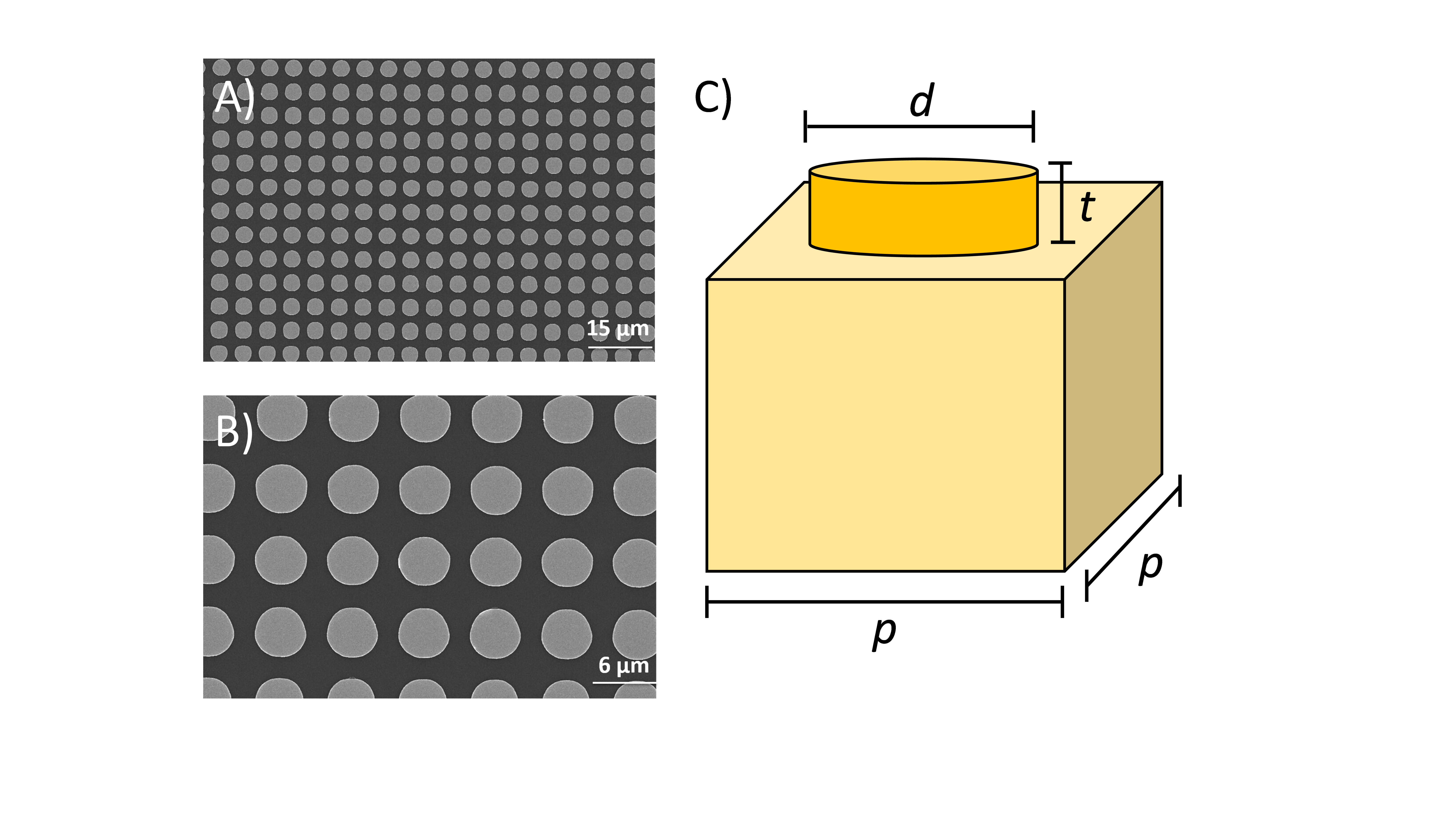
Figure 2. SEM images of the gold resonator, at A) 1000x magnification and B) 3000x magnification. The lattice constant was measured to be approximately 6 µm and the diameter is 4 µm. C) Three-dimensional schematic of the unit cell, where d = 4 µm, t = 100 nm, and p = 6 µm.
Reflection Spectra.
Reflection spectra were taken and simulated for gold resonators on a silicon substrate and gold resonators surrounded by VO2 film on a silicon substrate using FTIR. Both measured spectra used a gold mirror as the reference reflection, where the reflection of the gold mirror was considered to be 100%. The measured reflection spectrum for the gold resonator demonstrated a peak of 83.2% reflection at a wavelength of approximately 21.2 µm, less than 1 µm away from the simulated resonance value of 22 µm (Figure 3A). The reflection spectrum for the gold resonator with VO2 film was taken for the initial semiconductor state (21.4 °C), metal state (85.6 °C), and the semiconductor state upon cooling (21.3 °C). The semiconductor state exhibited a peak of 84.9% reflection at 21.4 µm and the metal state exhibited a flat reflection spectrum (Figure 3C). There was a maximum difference of approximately 20% between the reflection of the semiconductor state and metal state (Figure 3C).
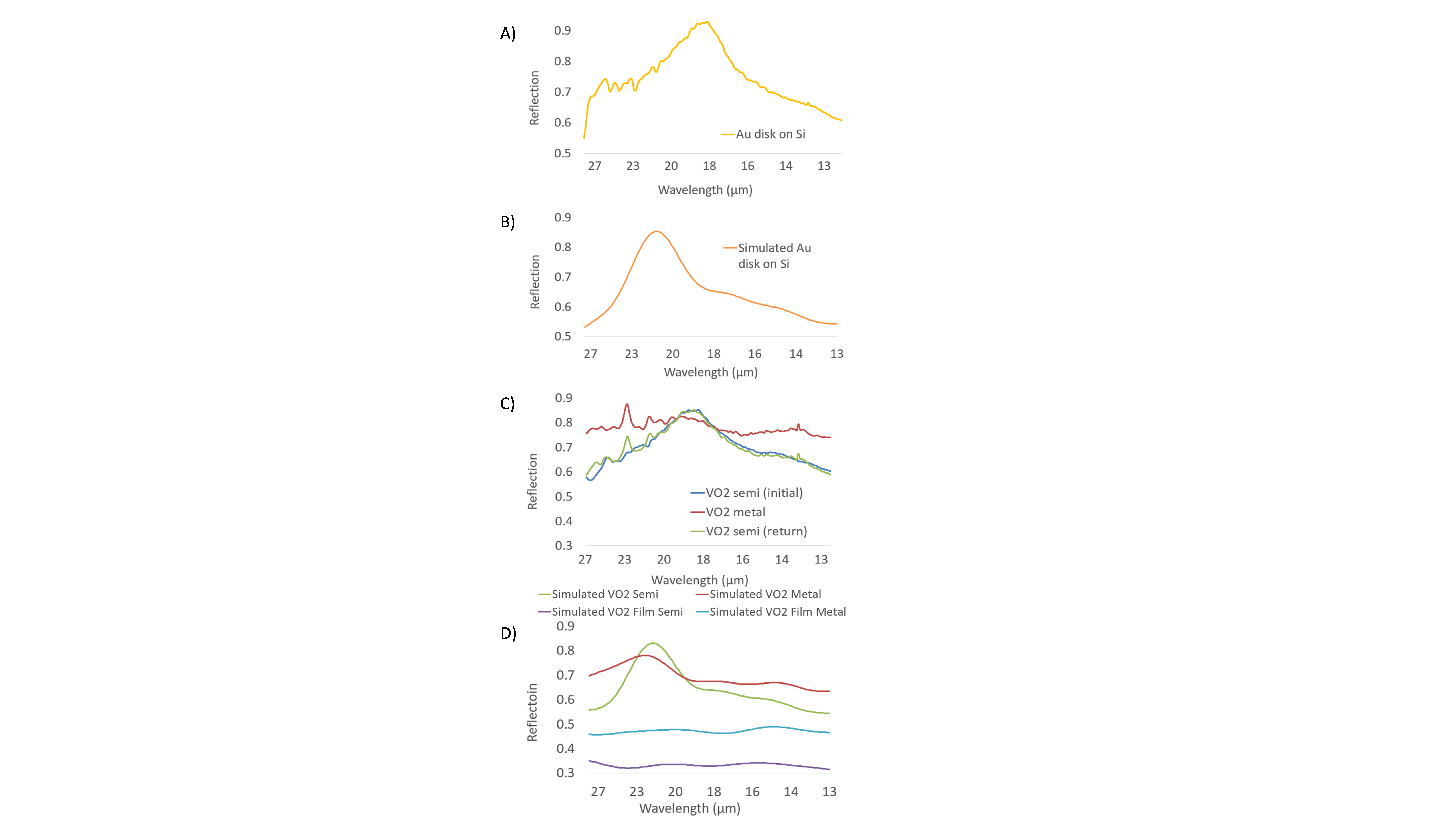
Figure 3. Measured and simulated reflection spectra for both gold resonators and gold resonators coated with VO2. A) Measured reflection for the gold resonator. There is a peak reflection of 83.2% reflection at approximately 21.2 µm. B) Simulated reflection for the gold resonator. C) Measured reflection for the gold resonator with VO2 surrounding medium. The semiconductor state (blue line and green line) exhibited an average peak of 84.9% reflection at 21.4 µm. The metallic state (red line) exhibits a relatively flat reflectance spectrum. D) Simulated reflection for the gold resonator with VO2 surrounding medium. The semiconductor state (green line), the metal state (red line), the semiconductor state of a VO2 film with no substrate (purple line), and the metal state of a VO2 film with no substrate (blue line) were all simulated.
DISCUSSION.
Reflection spectra were taken for gold resonators on a silicon substrate and gold resonators coated with VO2 on a silicon substrate. These spectra were used to determine the role of VO2 in the optical response of the material as well as its role in modulating the response. A change in peak reflection and resonant wavelengths at different temperatures indicates switchable VO2 and a tunable metamaterial. At a material’s resonant wavelength, transmission decreases and reflection increases. The reflection spectrum for the gold resonators had a peak reflectance of 83.2% at 21.2 µm, suggesting a resonance at that wavelength (Figure 3A). The reflection spectrum for the gold resonators in the presence of semiconducting VO2 had a peak reflectance of 84.9% at 21.4 µm, indicating the VO2 has a slight effect on the response of the bare gold resonators (Figure 3C). The reflection spectrum for the gold resonators coated in metallic VO2 did not exhibit an obvious resonance (Figure 3C). As the VO2 transitioned from the semiconductor state to the metal state, the reflection spectra flattened as the film became an unstructured metal with the VO2 masking the gold resonators. The peak reflectance experienced a slight decrease due to the fact that metallic VO2 has more loss than gold. The reflection spectrum of the system returned to its initial state upon cooling, indicating a reversible process (Figure 3C). Based on the difference between the semiconductor and metal reflection spectra, the VO2 metamaterial was tunable with the use of temperature. The measured reflection spectra agreed with the simulated reflection spectra for both the gold resonator (Figure 3B) and the gold resonator with VO2 film (Figure 3D).
The realization of a tunable metamaterial in this project is supported by previous studies. For instance, Zheludev and Kivshar demonstrated 20% modulation in temperature activated VO2 nanostructures in the terahertz range, supporting the conclusion that reflection modulation indicates switchable VO2 [12]. Zheludev and Kivshar performed experiments in the terahertz range but also ran simulations in the infrared with results further supporting the findings in this project. Dicken et al. demonstrated switchable VO2 with gold when heating the sample to approximately 85 °C, supporting the likelihood of obtaining switchable VO2 at that temperature [13]. Dicken et al. used VO2 inserted between a sapphire substrate and gold, explaining the slight difference of reflection modulation. Huang et al. demonstrated 15-30% reflection modulation in a different metamaterial by using an electrical current as a switch, which accounts for the varying range of modulation [11].
While normal metamaterials are limited in applications due to their passive nature, tunable metamaterials have a broad range of applications due to their adaptability. Tunable plasmonic metamaterials can be applied to antennas, lenses, and filters as supported by this work and the work of others [6]. Many devices are limited by size constraints, and integration of tunable metamaterials into electronic and optical devices could greatly reduce size while preserving and extending functionality [6, 11]. Tunable metamaterials can also be utilized for beam steering, dynamic holograms, ultrathin lenses, and spatial light modulators [6, 7, 11].
CONCLUSION.
Metamaterials are engineered materials that allow for unique manipulation of light and provide more engineering freedom than naturally occurring materials. Furthermore, active metamaterials open the door to novel applications that are not possible with the use of passive metamaterials. In this project, a tunable VO2 metamaterial was realized in the infrared. Reflection spectra were measured for both the semiconductor and metal state of the VO2 to confirm that varying optical properties occurred at different temperatures. Changing and manipulating the optical properties of a metamaterial in the infrared could lead to perfect absorbers, dynamic holograms, nanoguiding, beam steering, spatial light modulators, infrared camouflage, and cloaking [1-3, 6, 7, 12].
ACKNOWLEDGMENTS.
I would like to thank Dr. Jason Valentine for allowing me to work in his lab and for providing guidance throughout this project. I would also like to thank Zhihua Zhu for being my mentor and working closely with me. Finally, I would like to acknowledge The School for Science and Math at Vanderbilt for this opportunity and their support, especially Dr. Angela Eeds.
REFERENCES.
- N. Yu, et al. Light propagation with phase discontinuities: generalized laws of reflection. Science. 334, 333-337 (2011).
- J. Valentine, et al. Three-dimensional optical metamaterial with a negative refractive index. Nature. 455, 376–379 (2008).
- Horisaki, et al. Phase-Shift Binary Digital Holography. Optics Letters. 39, 6375-6378 (2014).
- Liu, et al. Terahertz-Field-Induced Insulator-To-Metal Transition in Vanadium Dioxide Metamaterial. Nature. 487, 345-348 (2012).
- J. Wei, et al. New aspects of the metal–insulator transition in single-domain vanadium dioxide nanobeams. Nature Nanotechnology. 4, 420-424 (2009).
- J. Schuller, et al. Plasmonics for extreme light concentration and manipulation. Nature Materials. 9, 368-368 (2010).
- D. Gramotnev and S. Bozhevolnyi. Plasmonics beyond the diffraction limit. Nature Photonics. 4, 83-91 (2010).
- L. Huang and H.T. Chen. A Brief Review on Terahertz Metamaterial Perfect Absorbers. Terahertz Science and Technology. 6, 28-39 (2013).
- S. K. Earl, et al. Tunable Optical Antennas Enabled by The Phase Transition in Vanadium Dioxide. Optics Express. 21, 27503-27508 (2013).
- L. A. Sweatlock and K. Diest. Vanadium Dioxide Based Plasmonic Modulators. Optics Express. 20, 8700-8709 (2012).
- Y. Huang, et al. Gate-Tunable Conducting Oxide Metasurfaces. Nano Letters. 16, 5319-5325 (2016).
- N. Zheludev and Y. Kivshar. From metamaterials to metadevices. Nature Materials. 11, 917-924 (2012).
- M. Dicken, et al., Frequency tunable near-infrared metamaterials based on VO2 phase transition. Optics Express. 17, 18330 (2009).
Posted by John Lee on Tuesday, December 22, 2020 in May 2018.
Tags: infrared, metamaterial, tunable, vanadium dioxide